SEALSQ, WISeKey, and Canton of Jura Execute MoU for CHF 40–60M ($48.7M–$73M USD) Post-Quantum Semiconductor Personalization Hub
quantumcomputingreport.com

SEALSQ, WISeKey, and Canton of Jura Execute MoU for CHF 40–60M ($48.7M–$73M USD) Post-Quantum Semiconductor Personalization Hub

SEALSQ Corp, its parent WISeKey International Holding Ltd, and the Swiss Canton of Jura signed a Memorandum of Understanding to create the Jura Post‑Quantum Semiconductor and Cybersecurity Center. The public‑private partnership will invest CHF 40 million to CHF 60 million over six years to develop regional expertise in personalizing, testing, and certifying hardware‑embedded post‑quantum cryptography. The center will use SEALSQ’s QS7001 Quantum Shield microcontrollers, which run NIST‑standard ML‑KEM and ML‑DSA lattice algorithms, and will support defense, aerospace, and critical infrastructure sectors. [...]
Taming Heat at the Nanoscale to Satiate Energy-Hungry Artificial Intelligence
semiconductor-digest.com

Taming Heat at the Nanoscale to Satiate Energy-Hungry Artificial Intelligence

Korean University researchers have engineered a “double‑confined” phase‑change memory cell that layers antimony telluride with nickel ditelluride and molybdenum ditelluride. The design confines heat to specific regions, allowing two distinct data states to be written sequentially without disturbing the underlying material. This architecture reduces reset energy by up to 76 % to 115 pJ, speeds switching to 50 ns, and extends endurance beyond one million cycles. The thin layers can be deposited with existing sputtering equipment, making the technology scalable [...]
Intel CEO Lip-Bu Tan on the one thing troubling his customers the most: I think in terms of the AI, the biggest challenge is…
timesofindia.indiatimes.com

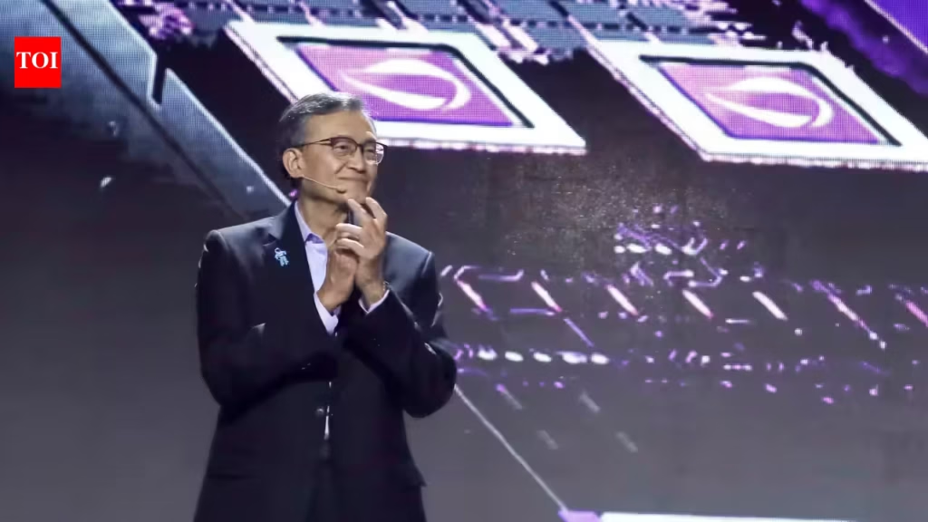
Intel CEO Lip-Bu Tan on the one thing troubling his customers the most: I think in terms of the AI, the biggest challenge is…

Intel CEO Lip‑Bu Tan warned that memory scarcity is now the primary obstacle for companies building AI infrastructure, citing a five‑to‑seven‑fold rise in memory prices and limited production that forces project delays. Speaking at Splunk’s .conf26 in Denver, Tan explained that demand for high‑bandwidth memory (HBM) from Nvidia and AMD accelerators has outstripped the output of Samsung, SK hynix and Micron, prompting a shift of existing lines to HBM and reducing capacity for standard DRAM. He relayed industry [...]
Nordic nRF54LC10A SoC expands nRF54L series for cost-sensitive IoT
electronicsweekly.com

Nordic nRF54LC10A SoC expands nRF54L series for cost-sensitive IoT

Nordic Semiconductor unveiled the nRF54LC10A system‑on‑chip, targeting ultra‑low‑cost tags, trackers and smart‑home sensors. The device integrates Bluetooth LE, Bluetooth Channel Sounding, Thread, Zigbee and Matter, and offers the same security and software ecosystem as the higher‑end nRF54L series. It is built around a 128 MHz Arm Cortex‑M33 core with a RISC‑V co‑processor, 1 MB non‑volatile memory, 192 KB RAM, three SPI/TWI/UART interfaces and an ADC. Radio performance includes 4.0 mA receive and 5.8 mA transmit currents at 0 dBm, +4 dBm peak output, –97 dBm [...]
India’s Semiconductor Push Gains Momentum as SEMICON 2026 Draws Global Industry
aryanage.com

India’s Semiconductor Push Gains Momentum as SEMICON 2026 Draws Global Industry

India’s semiconductor sector received a major boost at SEMICON India 2026, inaugurated by Prime Minister Narendra Modi in New Delhi. The three‑day showcase at Yashobhoomi attracted over 40,000 visitors, 400 executives, 150 speakers and 600 companies from 52 nations. More than 50 memoranda of understanding were signed, underpinning the government’s Rs 1,27,500 crore (≈ USD 15 billion) budget for the “Semicon 2.0” roadmap, which focuses on design, fab construction, ATMP/OSAT capacity, equipment, R&D and talent development. Union Minister Ashwini Vaishnaw announced investment pledges totalling roughly Rs 1 lakh crore (USD 11‑12 billion). [...]
Taiwan Steps Up Chip Race With New Advanced Packaging Park
brandiconimage.com

Taiwan Steps Up Chip Race With New Advanced Packaging Park

Taiwan inaugurated an advanced‑packaging industrial park in Kaohsiung on Monday, marking a major expansion of its semiconductor ecosystem. The Baipu Industrial Park, spanning about 88.7 hectares, will host two TSMC facilities: a technology‑validation laboratory and a talent‑training centre, slated to start operations in Q4 2029. Deputy Mayor Lo Ta‑sheng said the site will enable equipment and material suppliers to conduct research alongside TSMC’s packaging lines. President Lai Ching‑te highlighted the strategic role of advanced packaging in AI and [...]
Assam’s Semiconductor Facility Nears Operational Launch
gyanhigyan.com

Assam’s Semiconductor Facility Nears Operational Launch

Assam is on the cusp of launching its Tata Electronics semiconductor OSAT plant in Jagiroad, with trial runs now at roughly 25 % of capacity and commercial production slated for December‑January. The 592‑acre facility represents a ₹27,000 crore investment and is designed to output up to 48 million chips per day using advanced flip‑chip and ISIP packaging. Initial output will serve automotive, electric‑vehicle, telecom and consumer‑electronics sectors, while full‑scale capacity and a stable supply chain are expected to mature over [...]